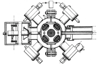
ref. 1
 ref. 1
|
Fred's Fusor
Ion Source |
|
Contents of this page Introduction This page describes the construction of an ICR helicon ion source. In the process of the construction of the basic Fusor we finally ended up with a cylindrical Fusor instead of the originally intended spherical Fusor. This was caused by the unexpected availability of a suitable T-shaped cylindrical vacuum chamber. Then we realised that this cylindrical vacuum chamber was also a good and suitable starting point for integrating an ion source. The purpose of the ion source is to investigate if we can use this set-up to increase the ion density in the Fusor for obtaining a higher fusion rate, which will be observed by a higher neutron output. A sub-project was initiated to construct a helicon ion source that could be integrated into the Fusor project. We discussed the characteristics of ECR/microwave sources and ICR helicon sources on our Theory webpage and concluded that a helicon source was a preferred choice. Please note with respect to your health that by using the described device on this webpage the maximum permissible exposure levels averaged over 6 minutes for the FM and VHF range from 88 to 108 MHz are an RMS electric field strength of 63.2 V/m, an RMS magnetic field strength of 0.158 A/m and a power density of 1 mW/cm2. Usually the preferred frequencies for operating ICR helicon plasma sources are chosen for ions with a charge of 1 at the natural frequency of 13.56 MHz in a magnetic field of 1.78T (and its harmonics) or at 2.45 GHz in a magnetic field of 86.6 mT, which is the natural frequency at which electrons gyrate and which is also a popular frequency due to the availability of cheap useable parts from microwave ovens. Most important fact is, however, that these frequencies are outside the RF frequencies that have been allocated to telecommunications. Introduction to the Theoretical Background The purpose of the helicon ion source is heating Deuterium gas to a plasma with a high density. The applied method of heating the plasma is by employing electromagnetic waves whose frequencies correspond to the cyclotron frequencies of ions and their harmonics. By launching electromagnetic waves at the ion cyclotron frequencies into the plasma a strong absorption of energy occurs because the ion cyclotron frequencies are one of the natural resonant frequencies of the plasma. The effect will be that a radiofrequent energy will be coupled into the centre of a magnetoplasma and that the energy will be transferred to the plasma particles (e.g. ions). Helicon waves are electromagnetic waves, which travel along magnetic field lines from an external aplied magnetic field. The name "helicon" has been derived from the effect that the electric and magnetic field of the travelling waves rotate in a helix trajectory. The advantage of an IRC helicon source as well as an ECR/microwave source is the fact that plasma heating occurs electrodeless. Both types of devices are low-pressure wave-heated plasma generators which produce a plasma density of 1010 - 1013 cm-3. The helicon ion generator is a device that produces electromagnetic waves propagating in magnetized plasma in the helicon mode (reference 1). The helicon wave is a whisler wave (or R-wave) propagated in (a) magnetic field(s) where the applied RF frequency is in the ω hierarchy range:
ωci = ion cyclotron frequency ωce = electron cyclotron frequency The choice of RF frequency and the applied magnetic field strength are flexible parameters ranging for RF from Mhz to GHz (though the absolute definition of RF is a wavelength ranging from 1 MHz to 500 Mhz) and for the magnetic field strength from 30 G to >1 kG respectively because the plasma production does not strictly require a resonant condition. The Lorentz force will cause an ion in a static magnet field to move in a circular pattern, a cyclotron motion. The cyclotron motion has an angular frequency ω equal to
For a given magnetic field strength B the angular frequency ω is given by
e is the elementay charge in Coulomb units (for a Deuteron = 1.60217733E-19 C) z is the number of negative or positive charges of the ion, dimensionless (for a Deuteron = 1) m is the mass of the ion in kg units (for a Deuteron = 3.3435860E-27 kg) B is the magnetic field strength in Tesla units. An electric exitation signal with a frequency f therefore will resonate ions with a mass-to-charge ratio of m/z given by
A uniform axial motion may be superimposed on the circular motion resulting in a circular curve in a three dimensional space, or a helix. When a uniform motion is superimposed perpendicular to the field (e.g. an electrical of gravitational field) a cycloid will result (reference 2). When a neutral gas is entered into the plasma chamber and the electrons in the gas molecules are energized by the RF wave, the electrons have the change of ionizing or exciting neutrals upon collision. When the electron temperature is low (< 5 -7 eV) excitations followed by de-exitations or permanence as a meta-stable state are major loss mechanisms. Only when high electron temperatures are achieved (> 10 eV) and when the ionization mean free path is smaller than the chamber length (λion << L) efficient ionization will take place. However, in addition the plasma chamber dimensions must be adequate for the desirable electromagnetic wave modes to propagate in it. In order to prevent plasma losses to the plasma chamber wall good electron magnetization will be required. This can be achieved when the electron Larmor radius is smaller than the tube radius (le << R) and when the Hall parameter is larger than 1 (ΧH >> 1). Note: Larmor radius: the radius of gyration; Hall ratio: the ratio between the electron gyrofrequency and the electron-heavy particles collision frequency. The ion cyclotron frequency for a given magnetric field strength therefore can be found by re-arranging the terms of equation IV to
For a more comprehensive overview of the helicon theory and plasma dynamics we refer to reference 3 and reference 4.  Components Plasma Chamber For the plasma chamber we will use a long glass tube with a small diameter. The preferred material is quartz glass as it is non-conductive and heat resistent up to 1450ºC and it has an exremely low coefficient of thermal expansion, about 5.5×10⁻⁷/°C (20–320°C), but sometimes borosilicate glass (max. temperature 600ºC) is also used, which may be possible because the plasma is heated under low-pressure (vacuum) conditions and the applied magnetic field keeps the plasma away from the glass walls by means of confining the plasma because a plasma is a diamagnetic medium. Nevertheless, some heat is exposed to the tube walls coming from ions and electrons reaching the wall, depositing their energy and recombining. For more details see further on this page. For our purposes we have acquired a fused quartz tube with dimensions 1500 mm length, 16 mm I.D. and 12 mm O.D (60" LG x 5/8" OD x 1/2" ID) (image 1):  Image 1: Quartz tube (source: Supplier) Our quartz glass tube was a lucky find as the dimensions of an outer diameter of 16 mm and an inner diameter of 12 mm make it possible to apply EU standard brass fittings and standard vacuum fittings for creating the inlet port for feeding of Deuterium gas as well as a vacuum connector. See the next paragraph about the vacuum connections. The acquired tube is far too long for our purposes and therefore we have cut off a section with a length of 150 mm by using an electric tile cutting machine. The tile cutting machine is the only instrument provided with water cooling and a diamond saw blade, which can make a decent cut in quartz glass. After the cutting job and after carefully drying the tube from adhering water, the quartz glass endings are heated in a propane/oxygen torch flame for melting the quartz glass cut surfaces to a smooth surface, which increases the strength of the tube endings and prevents from spontaneous cracking. The length of the tube and the diameter of the tube constitute an aspect ratio (diameter to length) of 0.11, which is within the typical range used for helicon plasma sources (reference 5)  Vacuum Connections The vacuum tight Deuterium inlet into the quartz tube is made by means of a Henco transition coupling 16 mm x 1/2" with O-ring (image 2):  Image 3: Henco transition coupling 16x½"with O-ring (© Henco) The Henco transition coupling consists of nickel plated brass and has been designed for coupling copper tubes, but can also be used (with some care) on quartz glass tubes too. Copper tubing will permit some compression for a tight fit but quartz glass doesn't. This means that tightening of the large swivel nut (at the left in the image, with an opening diameter of just over 16 mm) should not be done too heavily as the quartz may crack. Additionally, the compression ring (internal diameter just over 16 mm) should not be permitted to squeeze directly onto the quartz glass surface. A double layer of PTFE-tape under the compression ring is recommended. The fact that the coupler has an O-ring part (i.e. two O-rings at a small distance of each other) with an outer diameter of 12 mm that fits tightly into the inside of the quartz tube is essential for preventing cracking of the tube and to ensure a vacuum tight fitting. Though we are not in favour of using grease in vacuum systems it is advised here to grease the O-ring slightly with a good quality vacuum grease to faciliate easy sliding into the quartz glass tube. The ½" threaded stub at the end of the coupling (at the right of the image) will be closed with a ½" brass end-cap (identical to image 6) by using PTFE-tape. In the center of the end-cap a 1 or 1.6 mm diameter hole has been drilled to accommodate either a stainless steel O.D. 1 mm injection needle or a length of 1.6 mm OD stainless steel HPLC tubing, which has been brazed into the drilled hole. The needle or HPLC tubing acts as the Deuterium gas inlet and protrudes into the quartz glass tube beyond the metal parts of the coupling. The opposite side of the quartz tube, where it enters into the Fusor, has a vacuum tight connector which holds the quartz tube by means of an O-ring in a vacuum tight closure as shown in image 4:  Image 4: Glass tube to KF25 NW vacuum connector (source: Supplier) The connector in image 4 is unfortunately only available for KF25 NW, which is too large for our quartz tube. Therefore we have made a similar connector by using a KF16 NW to ½"BSP thread connector (image 5):  Image 5: Dimensions KF16 NW to ½" BSP connector The dimensions in image 5 are: A = 30mm / 1.2 inch, B = 20mm / 0.8 inch, C = 16mm / 0.7 inch, D = 40mm / 1.6 inch; the thread is "G" BSPP. The connector is completed with a suitable Viton O-ring and a ½" BSP "G" thread chrome plated brass nut cap (image 6), which gets a hole drilled in the center with a diameter of almost 16 mm, which is reamed to an almost tight fit around the quartz tube. Actually, we have drilled a hole of 10 mm diameter into the cap nut and than reamed it in a lathe up to 16+ mm. The reason for that action is that a conventional steel drill bit does not make perfectly round holes, which is better achieved by rotating the workpiece in a lathe and reaming the hole with a cutting chisel.  Image 6: ½" BSP Cap
Nut
By carefully tightening the end cap onto the KF connector, the O-ring enclosed inside the cap and around the quartz glass tube is compressed and expands radially towards the quarz glass tube and towards the brass cap wall thus ensuring a vacuum tight closure. A brass flat ring, fitting into the cap, may be needed in order to prevent rotational forces onto the O-ring when tightened, causing deformation and consequently vacuum leaks. Magnetic Field An axial magnetic field is applied by means of a series of permanent magents. The magnetic field has a number of functions:
For helicon discharges a magnetic field strength of 10 -100 mT is mandatory, which equals 100 - 1000 G. For our purpose of creating a dense deuteron plasma it should be noted that light ions e.g. from hydrogen or deuterium discharge require low magnetic fields in the order of 10 - 30 mT (100 - 300 G). For H2, D2, He, N2 and Ne a density jump is observed at an optimal external magnetic field B0.The measured plasma density np as a function of B0 peaks at a condition close to the lower-hybrid resonance in H2, D2, He, N2, and Ne. Magnets For our device we have chosen to use 20 pieces of annular magnets with dimensions of 27 mm outer diameter (OD), 5 mm thickness and 16 mm inner diameter (ID); all dimensions with a tolerance of ±0.1 mm. These magnets are made of sintered Neodynium-Iron-Boron with an outer coating of Nickel-Copper-Nickel. They have the following characteristics:
The field strength of these magnets can be calculated with an online calculator (reference 6) and the result is a field strength of 26 mT or 260 G. The magnets are concentrically arranged around the quartz glass tube, seperated by spacers at experimentally derived distances of 3 mm (see next paragraph). Another type of magnet that we could apply is a grade N45 magnet. It has dimensions of 25 mm OD, 20 mm ID and 3 mm thickness, is axially magnetised and has the following characteristics:
The latter magnets have a slightly weaker magnetic field but a larger internal diameter, which place them at a larger distance from the plasma tube. This should prevent warming up of the magnets and possibly passing the Curie temperature where all magneticity will be lost. Initially the idea was to use spacers made of 3-D printed ABS plastic but a calculation of the expected wall temperature made it clear that this material with a melting point around 200°C was not suitable: Ions as well as electrons may strike the wall with energies for ions of ±5 KBTe (the sheath drop) and for electrons of ±2 KBTe, i.e. a total of ±7 KBTe. The Bohm flux ½nKBTe is approximately the flux of ion-electron pairs striking the walls. When we neglect convective cooling and radiation from the inside surface we can make a conservative estimate by inserting this Bohm flux in the Stefan-Boltzmann law. For KBTe = 3 eV (for Argon gas) and n = 2E13 cm-3, the wall temperature might approximately become 860°C, well below the maximum temperature valid for quartz glass but far above the melting point of ABS. It remains however the question whether the plasma tube in practice will heat up to this temperature or not, as we know from literature many helicon thrusters which operate with borosilicate tubes. Conclusion: For placing the magnets concentrically around the quartz glass tube we may need to make use of rings cut from a non-magnetic metal, e.g. an alumina or copper tube with an ID just over 16 mm or by using plastic spacers at the outer circumference of the magnets. The magnets have a rather tight fit (ID = 16mm ± 0.1 mm) around the quartz glass tube (OD 16 mm), which might lead to cracking of the plasma tube when it gets heated by ion and electron impacts from sheath drop. However, the extremely low coefficient of thermal expansion for quartz glass of about 5.5×10⁻⁷/°C (20–320°C) causes no large dilatation and therefore might not lead to cracking of the quartz tube. It is all a matter of selecting suitably sized magnets and testing them for a sufficiently sliding fit around the quartz glass tube. Finally, in the worst case we might need to switch to magnets with a slightly larger diameter when our expectations will not be met. Measuring the Magnetic Field The magnets should be placed at specific fixed distances from each other to obtain the best possible almost homogenous magnetic field. Also we would like to know in an absolute value the strength of the magnetic field inside the quartz tube. For this purpose sophisticated magnetometers exist, but as we intend to do the measurements only once and because we are not interested in a highly accurate (calibrated) result we have considered constructing a simple magnetometer in our workshop. Different methods and schematics how to build a magnetometer can be found in the internet. As an example we have picked a very simple one (reference 7). However, we could not withstand the challenge and decided to build a slightly different model that uses an Arduino Micro-Pro to read out and process the signal (any Arduino version can be used). The main component in the schematic is the SS495B Honeywell Hall sensor, a miniature ratiometric bipolar Hall sensor with a linear range from -640 to +640 gauss (image 7): 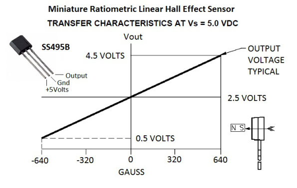 Image 7: Honeywell SS495B Hall Sensor With an Arduino Mini-Pro connect the +5V pin of the SS495B to VCC of the Arduino, the GND pin to GND and the Output pin to Analog input 0 of the Arduino. The Arduino source code can be found in reference 8. The readout of the Hall sensor can now be done in the serial print mode. The Arduino model type as used has a 10-bit analog to digital converter, which therefore maps input voltages 0 and 5 volt into integer values between 0 and 1023. The resolution between readings of the Arduino A/D-converter is therefore 5 volt divided by 1024 units or 4.9 mV per unit. When a higher resolution is required, than an Arduino Due or Zero can be used with the 12-bit ADC or a TI ADS1110 16-bit ADC can be integrated separately into the schematic. The resolution of the output of the Hall sensor in our setup is in a range from -640G to +640G, or a total of 1280 G units in a range from 0.5 V to 4.5 V, which is a range covering 4000 mV, where 4.9 mV is one ADC unit. Or: 1280 G units in 4000 mV divided by 4.9 mV, which equals about 1.6 G per ADC unit of 4.9 mV. With other words, our gauss readings are shown in resolution steps of 1.6 G. For our purposes, i.e. determining the magnetic field strength of our setup where the required magnetic field strength is between 100 to 1000G, this is sufficiently accurate and there is no need to change to a higher bit rate ADC.  Antenna The interface for delivering RF power to the plasma is formed by the antenna. The RF signal on the antenna causes waves to be emitted, which can be
Where possibility number 2 represents the desired situation, possibility number 3 can be quite disturbing to our neighbourhood especially when the applied helicon frequency is in the 27 Mhz or the 80 - 110 Mhz range, which are respectively the CB and the FM radioband. Radiation into free space therefore should be prevented by encapsulating the helicon plasma source in a (grounded) cage of Faraday. Possibility number 4 can occur with an unmatched impedance between power generator and antenna coupling causing the forward wave to be reflected back in the power line resulting in standing waves in the transmission line. Further about this issue can be found in the matching circuit paragraph. The simplest for of an antenna is the m = 0 type antenna, where m is the azimuthal mode number, i.e. an axisymmetric single loop antenna, which is known to have less wall losses compared to longer helical or Nagoya antennas and better coupling characteristics compared to other antenna designs. The m = 0 antenna is bidirectional (azimuthally symmetric) whereas the m = +1 helical antenna exites the wave in one direction as a right-hand polarized mode. Placement of the antenna is downstream of the magnets for better ionzation efficiency. For matching the antenna to the RF circuit it will be imperative to have an idea about the impedance of an antenna, which consists of a real part (the resistance) and an imaginary part (the reactance). The real part, the internal resistance of the antenna, can be neglected as it usually has a value of less than 1 mΩ. The imaginary part, the reactance of the antenna, can be calculated by XL = 2πfL
whereXL = antenna reactance in Ω f = frequency of the RF input in Hz L = inductance of the antenna in H The inductance of the antenna can be measured with a digital LC-meter as an approximative value. As an example we may find a value of 3.073E-2 µH (3.073E-8 H) for our m=0 antenna with a radius of 16 mm and a wire thickness of 1 mm. With an RF input of 200 MHz we can calculate a reactance of 38.62 Ω. In the antenna the current from an RF signal flows along the surface of a conductor (the antenna), which surface layer depth is called the skin depth. The skin depth of an RF antenna is given by  δ = skin depth in m µr = relative permeability (for copper = 1) f = the frequency in Hz (in our setup ≈200 MHz) ρ = the resistivity (for copper 1.68x10⁻⁸ Ω/m) As an example we can calculate the antenna skin depth for our 200 Mhz frequency as 4.6 µm, i.e. the current density drops off exponentially from the antenna surface in a layer with a thickness of 4.6 µm. It should be noted that according to the formula the skin depth decreases with an increasing frequency. A calculator for calculating a classical helix antenna can be found in reference 9.  Matching Circuit Once the antenna type and dimensions have been chosen, it must be matched to the transmission line from the RF power source. With "matching" is meant impedance matching between the RF transmission line impedance, usually 50 Ohm, and the antenna impedance which acts as a load impedance for the transmission line that carries the power signal to the antenna. The matching can only be done with the antenna fully functional and in place in the complete setup because everything around the antenna affects its performance. The radiated electromagnetic fields from an antenna interact with nearby materials and may change its frequency of operation and energy transfer into the plasma. Nearby objects to our antenna are the magnets, the spacers that hold the magnets at a certain distance, the quartz envelope, etc. The main purpose of the matching network is to maximise the forward power to the plasma and to minimise the power reflected back to the RF generator. The ratio between the forward power and the reflected power can be expressed as the standing wave ratio and it is a measure of the efficiency of the RF power transmission. The transmission line, usually a coax cable, but including adapters and connectors, to connect the RF-source to the matching network is a factor to be taken into account. When no adapters or connectors are present, the length of a transmission line is chosen as ¼ wavelength size, which is calculated by the formula λ= v/f, where v is the wave speed and f is the RF frequency. The wave speed is calculated by multiplying the speed of light (3x10⁸ m/s) with the velocity factor of the cable. For a RG 58/U coax cable we find a velocity factor of 0.66 and with our chosen RF frequency of 200 MHz we find a λ of 1.25m and therefore a ¼λ of 31 cm. When the ¼λ wavelength transmission line requirement is neglected the transmission line will generate reflected power that cannot be reduced by the matching circuit because it is generated "upstream". For the design of a (tuning) matching network a choice can e.g. be made from different possible types of LC-matching network, like the L-network, the Inversed L-network, the Pi-network and the Split-capacitor network. We shall take a look at the L-network and the Inversed L-network as the simplest forms of LC-matching networks. The L-network can be used when R1 > R2, where R1 is the impedance of the amplifier output (usually 50Ω) and where R2 is the impedance of the antenna (to be measured), as shown in image 8:  Image 8: L-network (© FRS 2017) The inductive reactance XL of this network can be calculated as: XL
= √(R1R2-R22)
The capacitative reactance XC of this network can be calculated as: XC = -R1R2/XL
For calculating the values of the inductor L1 and the capacitor C1 we make use of the general formula (below), but first we will consider the matching network when R2 > R1. In that case we will make use of the inverted L-network as shown in image 9:  Image 9: Inversed L-network (© FRS 2017) For the Inverted L-network, the inductive reactance can be calculated as: XL = R2√(R1/(R2-R1))
and the capacitative reactance XC of this network can be calculated as: XC = -R1R2/XL
For both networks the values for inductor L1 can be calculated as: L = XL / (2*π*f ) where f is the operating frequency. For both networks the values for capacitor C1 can be calculated as: C = 1 / (2*π*f *XC)
where f is the operating frequency.As mentioned earlier for solving the above equations we will need to know the impedance of the antenna system and measuring the antenna impedance requires expensive equipment, a network vector analyzer. A less costly investment can, however, be done in a VSWR meter, which will enable us to match the antenna impedance empirically to the transmission line. For that we will need a tunable matching circuit for which we introduce a variable capacitor and a variable inductor in the LC-network as shown in the schematics of image 10.  Image 10: Variable Matching Network (© FRS 2017) Details about this circuit can be found in reference 9. For the capacitor Cp in the matching circuit schematic we intend to make use of a Ducati air spaced variable capacitor with a capacity of 6 - 250 pF at a maximum voltage rating of 1500V (image 11).  Image 11: Ducati Variable Capacitor (Source: Supplier) For fine-tuning the variable Ducati capacitor we make use of a Jackson Bros 6:1 reduction ball drive (image 12).  Image 12: Reduction Ball Drive (Source: Supplier) As second capacitor Cs we will use a Jackson air spaced trimmer capacitor with a capacity of 4 - 30 pF at a maximum voltage rating of 750 V (image 13).  Image 13: Jackson Trimmer Capacitor (Source: Supplier) For the variable inductor Ls we will use an in-house built coil with an adjustable iron core. The iron core exists of the tip of a micrometer (image 14).  Image 14: Micrometer (Source: Supplier) The coil will exist of about six turns of 1 mm diameter copper wire around a Perspex jig with outside diameter of 7 mm and a bore of 6.5 mm. Inside the coil an iron core of 6.4 mm diameter can very precisely be positioned, fully or partially, over a distance of 28 mm. Insertion of the iron core, whitch has a high permeability compared to air, results in a greater magnetic field flux causing a higher inductance. The approximate inductance can be calculated, assuming that we have a coil with a radius r and a lenght l as L = (N2µA)/l
andµ = µrµo
whereL = Inductance of the coil in Henrys N = Number of turns in wire coil, straight wire is 1 µ = Permeability of core material (absolute, not relative, 1.25663753x10⁻⁶ for air, 6.3x10⁻³ for iron) µr = Relative permeability (dimensionless, 1.00000037 for air, 5000 for iron) µo = 1.26 x 10⁻⁶ T-m/At (permeability of free space) A = Surface area of coil in square meters or πr2 l = Average length of the coil in meters Suppose, we have a coil of 5 turns copper of 1 mm diameter with 1 mm between the windings and an inside diameter of 7 mm, than our coil has an outer diameter of (7 + 1 + 1) = 9 mm and a length of (4x(1+1)+1) = 9 mm. With no iron core we will have an open air core and by applying the formulas we find an approximate inductance L of: (52 x 1.25663753x10-6 x π x (4.5x10⁻³)2) / 9x10⁻³ Henry, which equals 222 nH. With an iron core fully inserted and applying the formulas we find an approximate inductance L of: (52 x 6.3x10-3 x π x (4.5x10⁻³)2) / 9x10⁻³ Henry, which equals 1.11 mH. Hence, by moving the coil in our example out and in the core we can change the inductance approximately between a value of 222 nH to 1.1 mH. This calculated result is more or less in the same range as the setup described in reference 10, where the variable coil has a measured variable inductance range of 100 - 160 nH, taking into account that in the article the core can only be inserted about halfway into the coil. The matching network is not a static device as it will require constant adjusting because the plasma itself has a dynamic impedance consisting of three components: capacitative, inductive and resistive.  VSWR Measuring In RF transmission systems the standing wave ratio is a measure for how efficient RF power is transmitted from the power source, through the transmission line, into the load, the antenna. SWR is the ratio between the transmitted and the reflected waves. A high SWR indicates a poor power transmission into the antenna and a high reflected power, which can damage the equipment. SWR refers to a voltage ratio and is therefore expressed as a dimensionless VSWR number. In an ideal system voltage does not vary and in such a system a VSWR of 1.0 means that the ratio is 1:1, or with other words reflection is absent. This is rarely the case. An example of a suitable VSWR meter is shown in image 15: 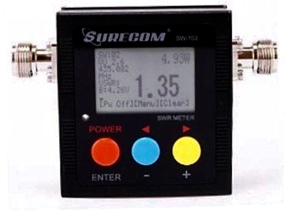 Image 15: VSWR meter (Source: Supplier China) This VSWR meter has an operational range between 100 and 520 MHz and an input power of 120W and measures the VSWR from 1.00 to 19.9 at an impedance of 50Ω.  RF power source The RF Power Source has a modular setup and consists of a number of rather inexpensive commercially available modules. The total amount of modules, however, will affect our budget quite intensively. The matching circuit, the antenna and some of the amplifiers (obtained as kits) are made in our workshop and for these items separate paragraphs can be found on this page. The layout of the modular RF Power Source for an arbitrary chosen frequency around 400 MHz is shown in the block schematic in image 16:  Image 16: Block
Schematic of the RF Power Source (© FRS 2016)
The inputs and or outputs in the block schematic are given in dBm, the power gain or power attenuation is given in dB. Total power output can be at a maximum of 100W. Impedances of all modules up to the matching circuit is 50Ω. A number of the modules may require cooling by forced air. For individually matching input and output power requirements, a number of digital step attenuators should be applied. This enables exact finetuning of an output signal to the input of the next module, thus preventing an oversteer of the amplifier causing distortion of the signal. It should therefore be noted that the choice and setup of the modules in theory should make sense, but in practice it is a hell of a job to match the components and to get a suitable final result, i.e. a fine-tuned RF output in the plasma without considerable losses. RF Function Signal Generator Any RF function signal generator can be chosen when it has a sine output ranging from 1 - 400 MHz or higher. The signal from such a function generator is quite weak and therefore several amplification steps are required before we can dump 100 W of energy into the plasma. We found a cheap old signal generator, working in the range of 0.14 to 112 MHz, a 1979 model Prüfgenerator "EP 105 BS a" by the manufacturing company of Dipl.-Ing. H.-G. Neuwirth, from Hannover, Germany, later bought by the company of Rohde & Schwarz, Munich (image 17). 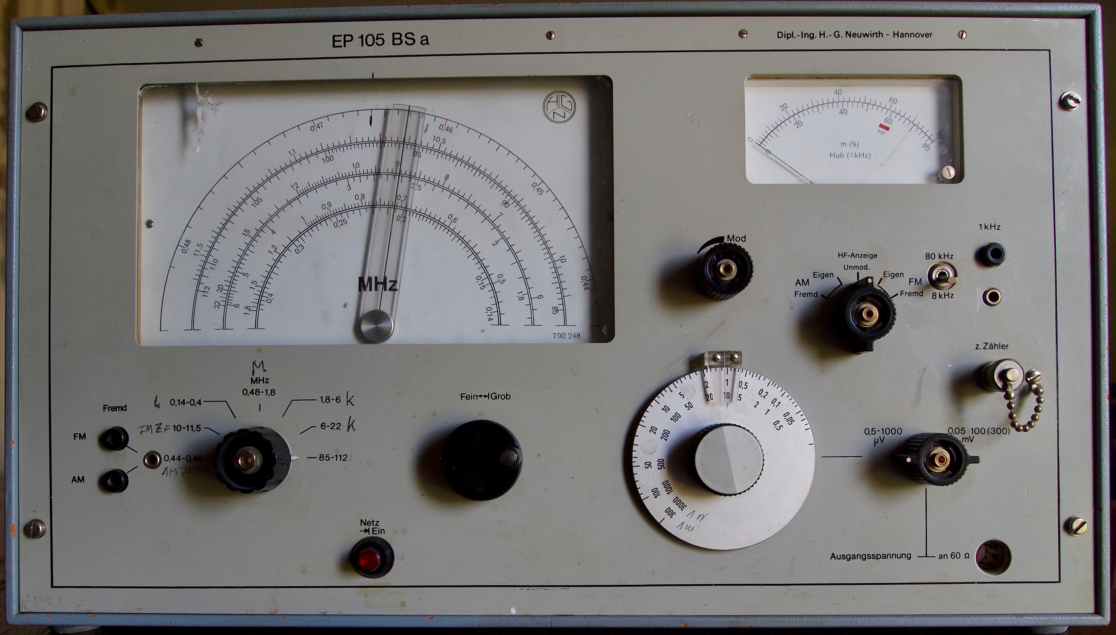 Image 17: Neuwirth HF Signal Generator (Source: Supplier) This signal generator has 7 Frequency ranges:
It is therefore our intention to perform a test with a cheap (around USD10) voltage controlled oscillator (VCO), commercially available in similar models suitable for generating a sine wave signal in the range from 70 - 200 MHz or in the range from 330 to 530 Mhz or even ranging from 515 to 1150 MHz (image 18): 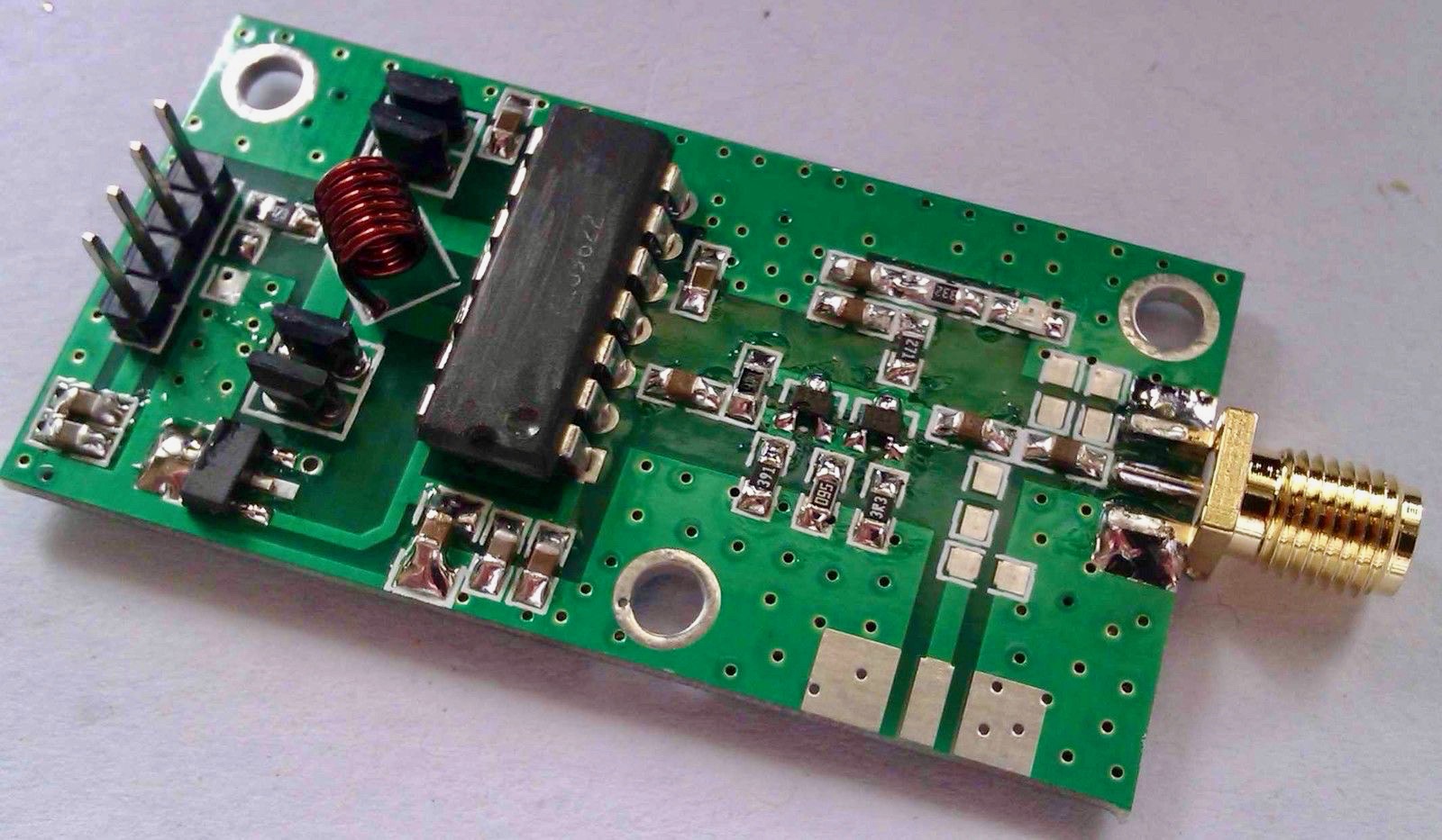 Image 18: Voltage Controlled Oscillator (Source: Supplier) The input voltage for the 70-200 MHz VCO is +12 V DC at about 50 mA, which is applied to the lower pin on the block of four pins at the left in the image. The two middle pins are ground pins and the top pin is the control pin to which a voltage ranging between 0 and +12 V DC has to be applied for obtaining a frequency output ranging from 70 MHz at 0V to 200 MHz at 12V. The output signal is 10 dBm (10 mW) with typical output harmonics of -15 dBc. A test measurement with 12V at the control pin resulted in a sinus wave with a maximum frequency of 197 MHz with a peak to peak voltage of 2.1V. A second VCO generator has a frequency range of 330 to 550 MHz (image 19): 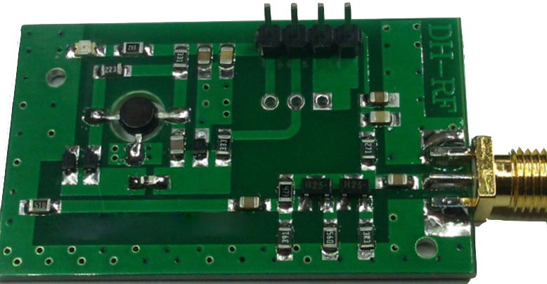 Image 19: VCO 330 to 550 MHz (Source: Supplier) The RF specifications are as follows :
 RF Pre-Amplifier The rather weak signal from the function signal generator needs to be amplified prior to further power amplification. For this purpose we may use a low noise broadband amplifier with a bandwith of 1 MHz to 930 MHz. With an input signal of 1 mW a gain can be achieved of 33 dB up to an output of 2.0 W. The output power is frequency dependent:
 Image 20: 1-930 MHz RF preamp 32 dBm (2W) (Source: Supplier) RF Step Attenuator The output power level is further controlled and adapted by a step attenuator between preamp and the broadband booster amplifier (image 21): 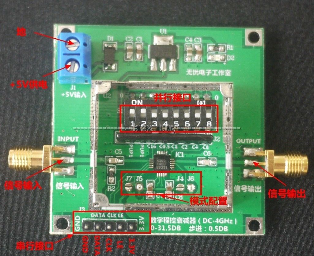 Image 21 RF Step Attenuator (Source: Supplier) The step attenuator offers a bandwith from 1 MHz to 4 GHz with an attenuation of max. 31.5 dB in 0.5 dB steps. The power supply required is 5 V DC. A digital model is shown in image 22: 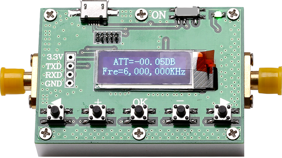 Image 22: RF Step Attenuator, Digital version with OLED Display (Source: Supplier)
RF Power Meter The RF Power Meter has a measuring range from 1 - 500 MHz at 1 nW - 2 W power input, with a measuring power range from -8- - +10 dB with a resolution of 0.1 dB (image 23):  Image 23: Power Meter (power setting) The power meter requires an input of 7 - 12 VDC at 50 mA. It can be applied between the broadband amplifier and the power booster. Additionally, RF power attenuation can be applied by adding or subtracting attenuation power in dB units (image 24): 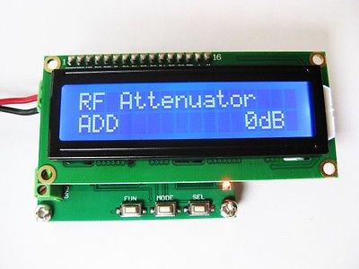 Image 24: Power Meter (attenuation mode) Between the circulator and the matching circuit we will apply a combined Power/SWR meter to measure the power output and the standing wave ratio for optimal antenna tuning. RF Power Amplifier The RF power amplifier (image 25) is used to convert a low power RF signal into a higher power, suitable to drive the antenna. 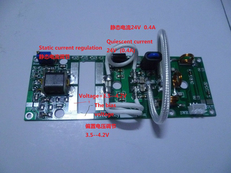 Image 25: RF Power Amplifier In combination with the VCO of the preceding paragraphs we shall try to perform a first experiment by testing the setup in combination with a 45W output 70 - 200 MHz power amplifier (image 26):  Image 26: 70 - 200 MHz Amplifier 45W (Source: Supplier) This amplifier has an input voltage of 24 - 26 V DC at 3 A. The maximum signal input is 1W and the maximum output is 45W. Cooling by a large heatsink and/or a fan will be required. As final power amplifier module we will make use of a kit for constructing a 400 - 470 MHz at 100W output amplifier (image 27):  Image 27: 400-470 MHz Amplifier 100W mounted on heatsink (Source: Supplier) This main power amplifier has an input power of 8 - 10 W and operates at a voltage of 24V at 7 - 8A. The output is 100W and care should be taken not to operate the amp without a load connected. A heatsink is required but it is not supplied with the kit. The main power amplifier requires an input power of 8 - 10 W and for that purpose we will need a pre-poweramp as shown in image 28:  Image 28: 350 - 480 MHz Pre-poweramp 13W (Source: Supplier) The pre-poweramp comes as a ready-for-use-module with forced air cooiling integrated. The supply voltage is 12 VDC with a stand-by current of 10-30 mA and an operating current < 3 A. The forced air cooling cuts in at 40°C, the input is -10 to 26 dBm (100 µW to 400 mW), the output power is 13 W, the frequency is 350 - 480 MHz with the second harmonic at -20 dBm. The dimensions are 70x40x10 mm, excluding SMA connectors. Units For comparing the specifications of amplifiers we may notice the use of different units in these specifications. Some useful formulas for calculating the specifications of amplifiers into different units are: Calculate power in dBm into Volts RMS: P(dBm) = 10 log10(v2/(R*p0)) where P(dBm) is the power in dBm; v is the voltage in volt; p0 is the reference point wattage of 1mW or 1x10⁻³W; R is the load impedance of usually 50Ω. Calculate power in Watts into dBm: P(W) = 1W ⋅ 10(P(dBm) / 10) / 1000 where P(w) is the power in Watt; 1W is the reference wattage of 1W; P(dBm) is the power in dBm. Calculate gain: GdB = 10 log10(W(output)/W(input)) where GdB is a dimensionless value; W(output) is output power in Watts; W(input) is input power in Watts.  RF Circulator The RF circulator or an RF isolator is used for blocking reflected power from the antenna circuit by dumping this power into the dummy load. It is rather difficult to find a suitable (used and cheap) circulator in the frequency range of 80 - 120 MHz VHF bandwith and for the applied power of 100 W; moreover they are somewhat bulky due to the required low frequency range. Most used RF circulators on the market appear to be designed for the GHz UHF bandwith and therefore can do with smaller dimensions. The principle of operation of a circulator, a three port ferro-magnetic device with the ports arranged in a triangle, is that it has directional properties from port to port. RF energy is directed from port 1 to port 2, but not to port 3, caused by ferromagnet coupling inside the circulator. This occurs on all ports, thus obtaining a directivity travelling in one direction around the triangle. The directivity (or "isolation") is measured in dB, e.g. a port to port isolation of 20 dB means that it conducts RF in one direction 100 times better than in reverse. Isolation, however, is only provided when the circulators are terminated, typically at 50Ω. As a passive device circulators can be designed and constructed as a waveguide (cavity), coaxial or stripline circulator. A stripline circulator usually is constructed with the coupling between the ports consisting of flat insulated overlapping terminated copper sandwiched striplines in a 120 degree angle position. The flat copper striplines are sandwiched between two discs of optimised ferrite. A permanent magnet imposes a strong magnetic field across the discs for generating the directivity. In some circulators internal matching networks may be present as L/C circuits or variable trimmer capacitors. When chosing a circulator near to the required frequency, such a matching network may permit to shift the operating frequency of the device and change the degree of port to port isolation. For tuning, always with the circulater connected in "reverse", it will be imperative to terminate all ports with 50 Ohms and then tune for maximum rejection of the signal at the required frequency, rotating through all three ports for tuning to the same. Never tune the circulator in the forward direction as this will not work! Our search for a suitable circulator made us find a used high power circulator, which came from army surplus and its working range is in the 200 to 400 MHz bands (image 29).  Image 29: Temex Circulator (Source: Supplier) It is a Temex brand device, though it is also marketed by Cobham Microwave, a model BB3007 with the following specifications:
Table 1: Circulator
Specifications
This three-port coaxial circulator is a so-called Y-junction circulator which uses ferrites in the presence of a magnetic bias field, in order to provide a non-reciprocal effect. If a signal is applied at port 1 it will emerge from port 2 with a loss characteristic, called the insertion loss (I.L), which in our circulator equals 0.70 to 0.80 dB. In the reverse direction there will be a leakage at port 3 from the incoming signal at port 1. This leakage, called isolation, is 14 to 17 dB below incoming power at port 1 in our ciculator. The lucky find of this circulator necessitates us to feed our ion source plasma with a frequency in the range of 200 to 400 MHz. RF Dummy Load The dummy load is a 50Ω Non-Nichrome resistive RF termination impedance resistor with a 150W power rating. It can be used up to a frequency of 3 GHz. The resistor will need to be attached to a large metal cooling block with a thin layer of thermal paste applied between the contacting metal surfaces (image 30): 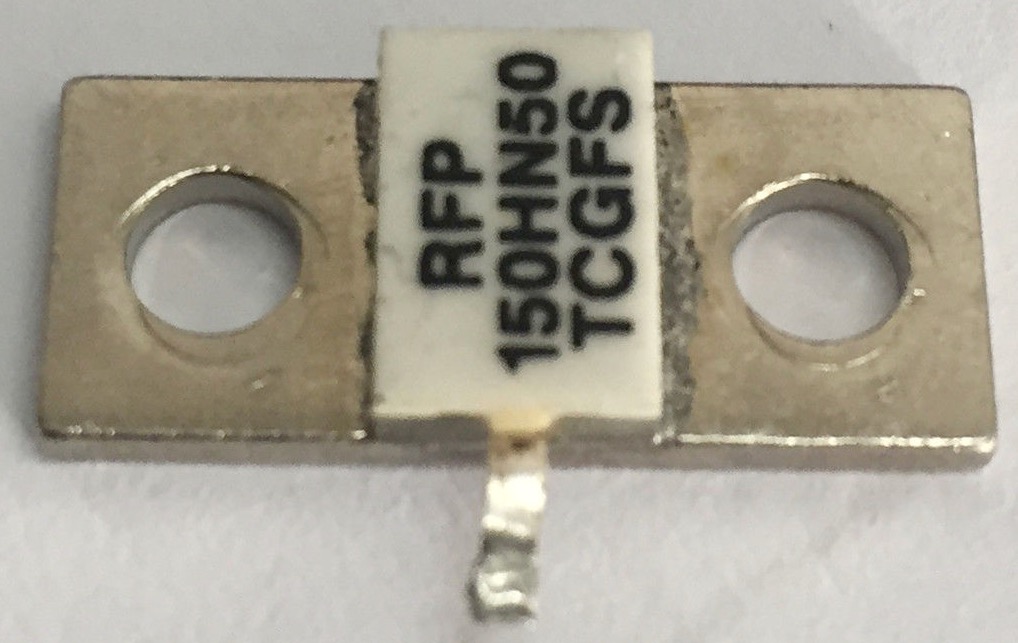 Image 30: RF Dummy Load 150 W These RF dummy loads also exist with integrated coax cable and SMA connector (image 31):  Image 31: RF Dummy Load with coax cable and SMA connector (Source: Supplier) Image 32 shows a standard LED heatsink with a capacity of 100W that can be applied with the dummy load:  Image 32: Heatsink for Dummy Load  Construction Assembling the VCO generator The 70 to 200 MHz VCO generator comes as a complete module. Nothing has to be assembled, except a voltage ranging from 0 to 12V for regulating the frequency output has to be connected. This is done by using a ten turns linear 100 kΩ potmeter (abritary choice because just at hand), which is connected as a voltage divider from the 12V input power to ground and with the wiper pin connected to the VCO frequency control input pin. The current through this 100k potmeter is 120 µA and the power dissipated is 1.4 mW. A potmeter of 10k would have suited as well. In addition to the 70 to 200 Mhz VCO1 generator, a 330 to 550 Mhz VCO2 generator will be used to extend the range of frequencies for better matching our existing RF circulator. This model also uses a 12V DC input power and 0 to 12V for setting the frequency. Therefore we decided to use both models constructed in one aluminium box together with the ten turns potentiometer with vernier, two switches and a LED control light as well as a frequency meter module for controlling the frequency as set. The aluminium box shall also have output connectors for 12V DC and 5V DC for powering additional modules, next to the 12V DC input connector. Image 33 shows the wiring diagram for the modules: 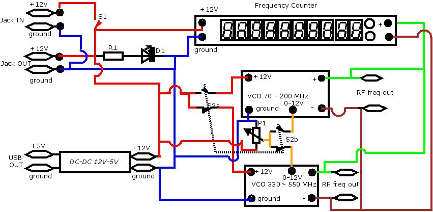 Image 33: wiring schematic for VCO modules (©FRS 2018) The wiring schematic shows both VCO modules, an 8-digit frequency counter module, model PLJ-8LED-C, a DC-DC converter from 12V to 5V with USB connector (basically the circuit board with components from a cigarette lighter usb power supply), an ON-OFF switch S1, a power ON LED D1 with resistor R1 (560Ω/0,5W, a double throw switch S2 for applying power to each VCO module, a ten turns potentiometer P1 with vernier dial for setting the VCO variable voltage, two SMA female output connectors, an input connector and an output connector. The components are placed with appropriate shielding in an aluminium box. For VCO outputs, coax cables should be used. The finished VCO generator is shown in image 34, for module VCO1 operating at 193,119.1 kHz, i.e. 193.1 MHz:  Image 34: Finished VCO generator (©FRS 2018) Assembling a 45W Power Amplifier The power amplifier of image 26 is sold on eBay as a kit named "DIY kits 45W 70-200MHZ power amplifier for FM VHF transceiver radio amplifiers". When ordering this kit it wll be a big surpirse to receive it and to find it without any schematic or instructions how to assemble the kit. Not even a link to such information is present on the (Chinese) seller's eBay auction page and neither on any of all other sellers pages! Because the pcb also has no printed info on it about the components, the lucky buyer finds him/herself stuck with about USD 20 less in the pocket and in the happy posession of a for the time being useless bag filled with components and a pcb with dimensions 100x50 mm (image 35).  Image 35: components of the power amp (©FRS 2018) By analyzing the contents from the bag we find the following:
Looking at the completed amplifier in image 26, where we count 18 soldered components, whereas we found in the bag 74 individual components, we may conclude that we have received a large surplus of components. The reason for it is probably courtesy as well as laziness from the supplier because the tiny SMD components get easily lost and it is easier for them just to cut off a certain strip length of these components, which cost next to nothing. Another observation is the different look of the wire coil. In the picture we see a clockwise wound coil with 9 or 10 turns of copper wire, whereas the coil in the supplied kit has 3 turns. Moreover, the supplied wire coil has been wound into the "wrong" anti-clockwise direction, making it more difficult to solder it onto the pcb. By contacting the seller a link was received for downloading the schematic for the power-amp (reference 11) but it can also be downloaded from here. Note: a few weeks later (when we had finished our reverse engineering and started to assemble the kit) we kindly received from a forum member the missing layout schematic with component values indicated. It gave us a hint how to choose the values for the components but nothing more than that because all values are given in more or less wide ranges. Almost immediately we noticed that the open air wire coil as supplied with the kit is not the one as shown in images. According to the component layout the coil should be 0.6*4*10T, or 0.6 diameter wire (23 gauge SWG), 4 mm coil diameter and 10 turns of wire with a calculated inductance of 200 nH, whereas we received a coil with 3 turns of wire and a larger diameter of 10 mm with a calculated inductance of about 96 nH, as mentioned before. However, we expect that the wire coils as supplied probably will do the job as required and therefore can be used in the power amp. The layout is shown in images 36 and 37 and it can now be downloaded from here.  Image 36: Component layout power amp (© Supplier)
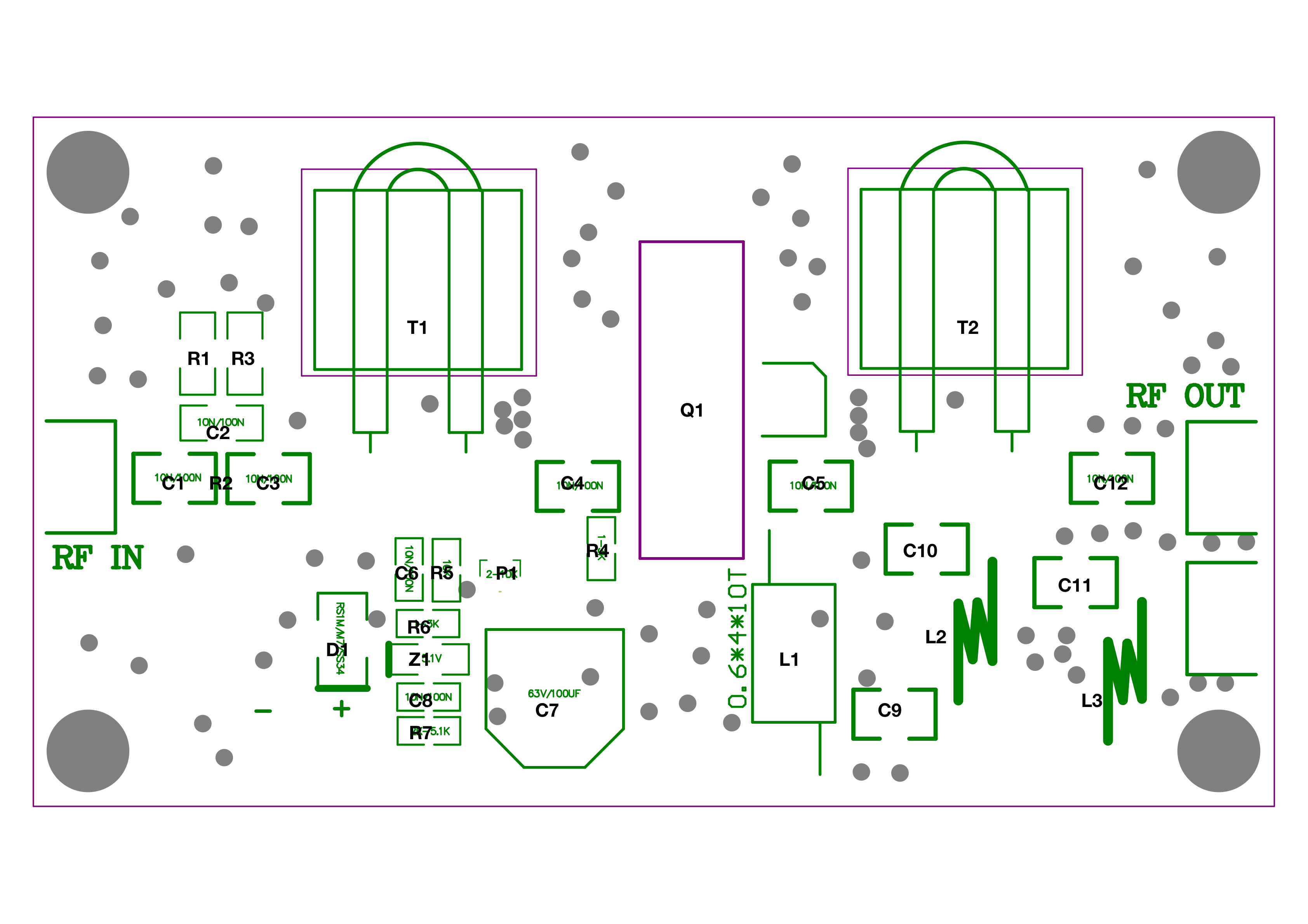 Image 37: Component layout with component numbers, referring to image 37 According to the schematic the power amp is a class AB amplifier with a quiescent drain current of 30 mA. Unfortunately, another problem arises now because no values for the components have been listed in this schematic! We found ourselves forced to apply some reverse engineering. Therefore we decided to draw the same schematic but now with all components numbered in order to facilitate discussing the particulars of the design characteristics (image 38).  Image 38: Schematic
for 45W 70-200 MHz Power Amp (©FRS 2018)
(Including component values from the supplier's layout schematic added after finishing the project) The attenuator formed by resistors R1, R2 and R3 is a so-called Pi-pad attenuator, which can be used as a fixed attenuator between equal impedances or for impedance matching between unequal impedances. In our case, where we will apply an input at 50Ω with an input power less or equal to 1 W no impedance matching or attenuation will be required and therefore we will enter the input signal through a wire jumper for R2 (leave out R1 and R3) and the coupling capacitor C1 and C3, leaving out C2. With values of 100 nF for each ceramic capacitor the input line will be suitable for VHF/UHF frequencies. The function of the capacitors is to reduce noise (ripple) from the previous section or picked up by the transmission line connecting to the previous section. Note: When we enter the values for attenuation (= 0 dB) and an impedance of 50Ω for the signal entering into a Pi-pad calculator as found available on the internet, than we will find values of infinity (i.e. open circuit) for R1 and R3 and a value of 0.00 for R2 (i.e. zero resistance or: bridge with a wire or small blob of solder). The LPF (low pass filter) section consists of (probably, though we could not measure a resistance over the "coils" on the bare pcb) two microstrip etching transmission lines (L2 and L3) and three capacitors C9, C10 and C11, making up here a 5-component so-called Chebyshev Pi-LC low pass filter. The LPF is meant to suppress frequency harmonics in the output. Something is to be said about the possibility that the lines are not printed coils, because depending on the cut-off values for the LPF we would require different values for the inductors, i.e. other than pre-fixed in an etched coil. Suppose now that we would like to calculate the values for L and C in the LPB in the schematic, than we can make use of reference 12. Prior to that it would make sense to measure the inductance of both microstrip etching transmission lines on the bare pcb board to give us an indication for which cut-off frequency we are looking. Should we measure no inductance or resistance than we must assume that air coil inductors will have to be applied, of which we probably erroneously have received one with a value of 96 nH in the supplied bag of components instead of the required L1 conductor. However, this all does not matter because this output mode is of no interest for our purposes, we only will make use of the "no-LPF SMA output" connector through the series coupling capacitor C12. Its function is to block DC and the value of 100 nF will block frequencies below about 10 kHz and it will let pass frequencies above about 10 kHz. Rather mysterious components are the two pieces of semi-rigid RF coax (0.085" diam.), which are each to be placed into a binocular ("pig nose") ferrite core. Most probably the function of the components are meant as wide band transmission line transformers for transforming up the input impedance of 50Ω to a higher value of a factor 4. This might have to do with the fact that the input impedance of the power fet appears to be rather low for HF frequencies. We shall just solder them onto the pcb as indicated in the schematic and not further worry about it. Bending the semi-rigid coax into a U-shape, fitting into the binocular ferrite core, should be exercised with the utmost care. A mandrel or jig for the required radius should be used at all times and bending to the required radius should be performed in steps from a larger radius to smaller radii until the required radius is obtained. Also soldering wires to the outer metal mantle should be exercised with care: fast and not too hot in order not to damage the dielectric inside. That leaves us finally to describe the biassing circuit for the mosfet transistor. The idea that we will follow is to use the (values of the) supplied components as a starting point for "reverse engineering" the bias circuit. Only when calculations show that for a component a different value should be used for better performance than we will discuss that and change the component. For taking a closer look at the bias circuit we have drawn the circuit for it in a somewhat different arrangement of components, however it is a part from and equal to the schematic in image 32, with the same numbering of components (image 39). 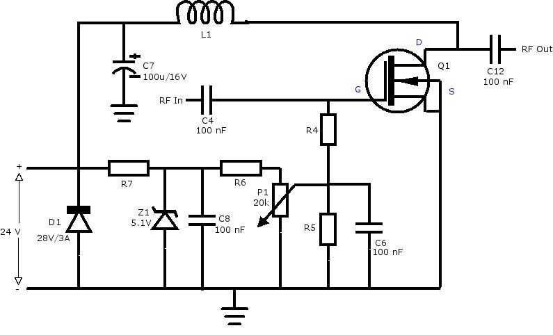 Image 39: Bias circuit (©FRS 2018) When we start at the power entrance side of 24V DC/3A, the first component is D1, a Schottky Diode rated at 28V/3A. Its function is to protect for faulty connection (reversed polarity) of the 24V power supply, but this shall only work when the power supply has a current limiter falling within the characteristics of the diode. If not, the diode shall turn into smoke when connected with the wrong polarity of the power supply. The next series of components are resistor R7 with Zener diode Z1 rated for 5.1V. This combination of resistor and Zener diode acts as a voltage regulator for the bias circuit. With R7 at a value of 2 kΩ the bias circuit voltage will be kept more or less constant at the Zener voltage of 5.1V, depending on the combined resistive load of R4, R5, P1 and R6. Capacitor C8 with a value of 100 nF is for reduction of noise from the Zener diode. Resistor R6 in series with P1 offers a threshold resistance value to ensure that the current remains at a certain value, even when P1 is rotated to zero resistance. The value for R6 is 2k with a value of 20k for P1 (which according to the schematic layout has to be set at 2-10k). Decoupling capacitor C6 with 100 nF value AC connects R4 to ground. Resistor R4 at the gate of the Mosfet has been marked in the downloaded schematic as 51Ω but in the schematic layout as 1-3k. A 2k resistor is present in the assortment of components supplied with the pcb, but 51Ω is not present. We have used here a resistor of 49.9Ω ±1% and ¼W from our toolbox. That leaves us with a value of 10k for R5, connecting R4 to ground. The N-channel mosfet MRF9060M has a 1265-07 / TO270 case where the two strips with the holes are the source connector, the strip with a small corner cut-off (under the "D" in the image) is the drain and the strip opposite the drain is the gate (image 40).  Image 40: Pin layout of M9060M Mosfet (©FRS 2018) The datasheet for the M9060M can be downloaded from here. For assembling the power amp it is advised to start with the "rough" work first by marking the six holes on the heat sink for attaching the pcb and the power fet with M3x10mm size nuts. Drill the holes with a 2.5 mm drill and tap the M3 threads. Solder the components onto the pcb, starting with the SMA connectors, followed by the coax transformers. Strip the coax wires to the desired length, bend through the pig noses and solder them onto the pcb. Take care that the solder joints are without mechanical stress, i.e. use sufficient wire length and bend it to connect to the solder pads on the pcb. Next solder all analog components onto the pcb: the wire coil, resistors, potmeter and capacitors, then diode and zener, followed by the electrolytic capacitor. Solder only one terminal of the wire coil to the pcb. Finish with soldering the power fet to the pcb but first screw the pcb with the four corner nuts onto the heat sink after first applying a light coating of thermal paste between the ground plane and the heat sink surfaces. Then screw the two sources of the power fet with two M3 nuts onto the heat sink (apply thermal paste between source and heat sink) and finally finish with soldering the drain and the gate on the pcb (avoid mechanical stress). Finally the amp is than adjusted to the required quiescent drain current IDQ by placing a multimeter in the mA mode between the wire coil and the unsoldered connection to the pcb. Connect 24V DC to the amp and adjust with the potmeter until a reading of 30 mA has been obtained. Remove the multimeter and solder the remaining connection of the wire coil to the pcb. The power amp is now ready for use (image 41). 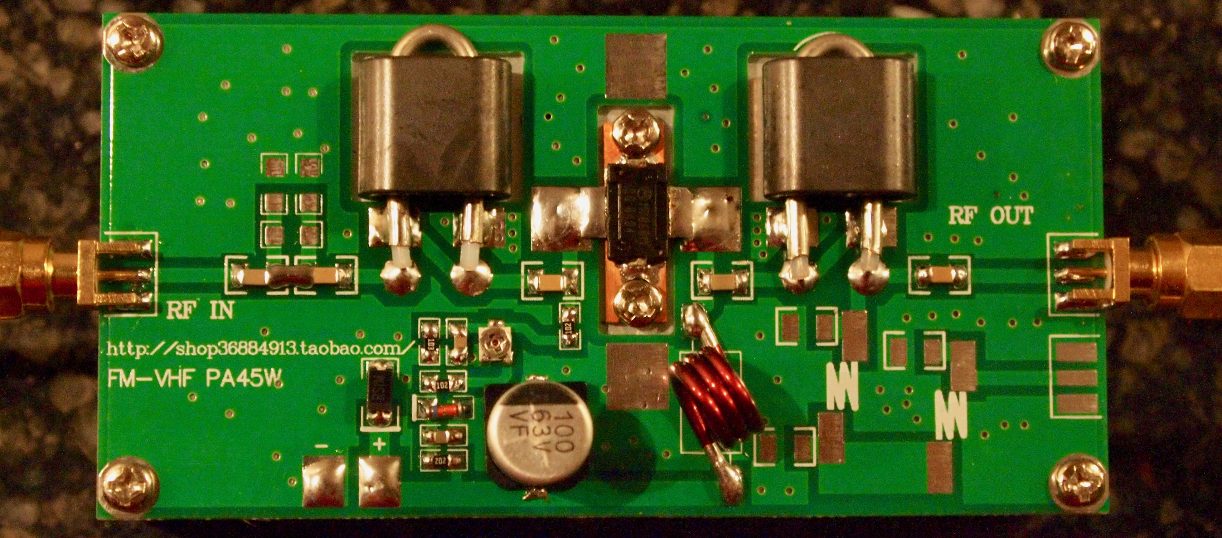 Image 41: The power amp finished (© FRS 2018) Assembling a 100W Power Amplifier The 100W, 400-470 MHz power amplifier of image 27 is sold on eBay as a kit (image 42)  Image 42: Kit for 400-470 MHz poweramp, 100W (© FRS 2018) Similar to the previous amplifier no specific information is supplied with the kit, except a component layout schematics with values for the components can be found on eBay (image 43).  Image 43: Layout 400-470 MHz poweramp, 100W (Source: Supplier)
The excellent pcb is shown in image 44: 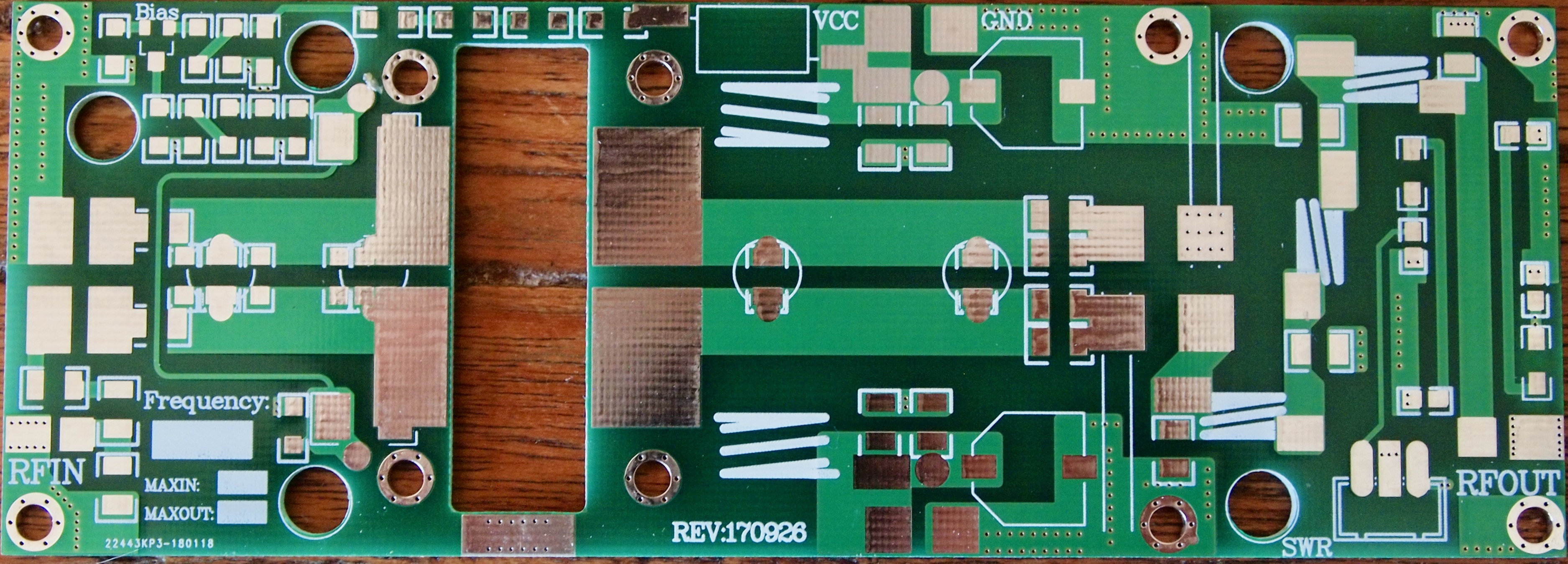 Image 44: PCB 400-470 MHz poweramp, 100 W (©FRS 2018) Image 45 shows the finished version of the amplifier:  Image 45: Finished Version 2 400-470 Mhz poweramp, 100W, mounted on a heatsink (source: Supplier) A schematic was retrieved from the internet (image 46) and it can also be downloaded from here.  Image 44: Schematic 400-470 Mhz poweramp, 100W (source: Supplier)
Evaluating the Kit: Prior to soldering the components onto the pcb all components need to be checked for presence and correct values. The kit contains a number of used components, such as the MRF186 RF Power FET and ten pieces of ATC capacitors. A used MRF186 FET costs about € 13.00 and a new one starts at € 40.00 whereas an ATC capacitor costs from € 0.65 to € 1.50 a piece. Taking into account that the compete kit is sold for € 30,17 including shipping from China, we can accept that used, refurbished components are being supplied. The amplifier has two impedance transformers consisting of calculated lengths of coax cables. Because the amplifier has been designed for ≈ 70 cm wavelength and therefore at our operational frequency of 400 MHz or 74.948 cm the two λ/4 wave coax cables should ideally have lengths of ¼*74.948*0.66 cm (where 0.66 is the velocity factor for the type of coax) equalling 12.4 cm. However, the supplied lengths are respectively 11.9 and 12.2 cm and we should possibly consider replacing them with correct lengths. Because the amplifier has been marketed for a frequency range of 400-480 Mhz, the quarter wave stubs should consist of lengths varying between 12.4 to 10.3 cm and therefore the supplier of the kit should have supplied two coax lengths of 12.5 cm in order to permit the user to cut the lengths at the required sizes for his/her preferred frequency of operation. The Zeners should be checked to be 5.1V. Evaluating the Schematic: The schematic is for its setup not much different from the schematic of the previous amplifier:
The attenuator is straight forward as we do not intend to attenuate the signal here. Therefore, the signal enters directly at 50Ω through two capacitors in series with values of 10nF, connected to the inner core of a coax stub. The bias circuit is to be soldered onto the pcb first and prior to further adding components a test should be made by putting 24 V DC on the circuit and measuring the output voltage of the bias circuit. After completion the quiescent current should be adjusted with the potmeter to about 300 mA. Personal reminder: Nieuwe ingangstrimmers 5-25 pF plaatsen en ook nog een trimmer tussen de uitgangen van de FET (Tronsor 19 pF) later vervangen door een ATC van 20 a 25 pF; nu ruim 100 watt per eindtrap op de meter ..( 9 watt in , 28 volt ) en dat met een redelijke ingangs SWR van 1: 1.5 Tussen de twee drains van de fets heb ik een condensator van +/- 25 pf gezet ik kreeg toen een veel betere ingangs SWR en ook wat meer output ... het was trial en error. Er zal denk ik nog wel een extra LPF achter moeten .. maar eerste QSO is gemaakt er loopt per dubbele FET iets van 650 mA ruststroom nabouwers succes en denk erom alle onderdelen nameten RF Tap For measuring the waveform and output of power amplifiers we have constructed a 200W, 40 dB RF-tap (or non-directional coupler) as designed by Loftur E. Jónasson, according to reference 13 (at the bottom of that link page). The RF-tap has a linear attenuation of about 40 dB from 1 MHz up to approximately 450 MHz, but beyond 500 MHz the signal starts falling apart. The schematic is as follows (image 47):  Image 47: 40dB RF-tap (©FRS 2018) For the choice of components as recommended we used for R1 and R2 metal film resistors of 1k and 3W, for R3 also a metal film resistor of 3W but 470R, all resistors in series, thus obtaining a resistance of 2470Ω. For C1 we used a short wire stub soldered in parallel with R1 for high frequency compensation. For R4 and R5 we used resistors of 100R and ¼W in parallel, thus obtaining a resistance of 50Ω. The choice of resistors enables power measurements up to 200W, with short bursts up to 400W. The 50Ω match against the wall of the enclosure, from the topmost connectors in the straight transmission line, is obtained by mounting between the two topmost connectors an unetched single sided pcb with dimensions of 1"x½" (25.4 mm x 12.7 mm). For the two topmost connectors we used female SMA connectors (simply because that is the standard in our RF system) and for the bottom connector we used a standard BNC connector for connecting an analyzer, scope or other equipment. All components are mounted in a Hammond 1490A aluminium die-cast box (image 48). 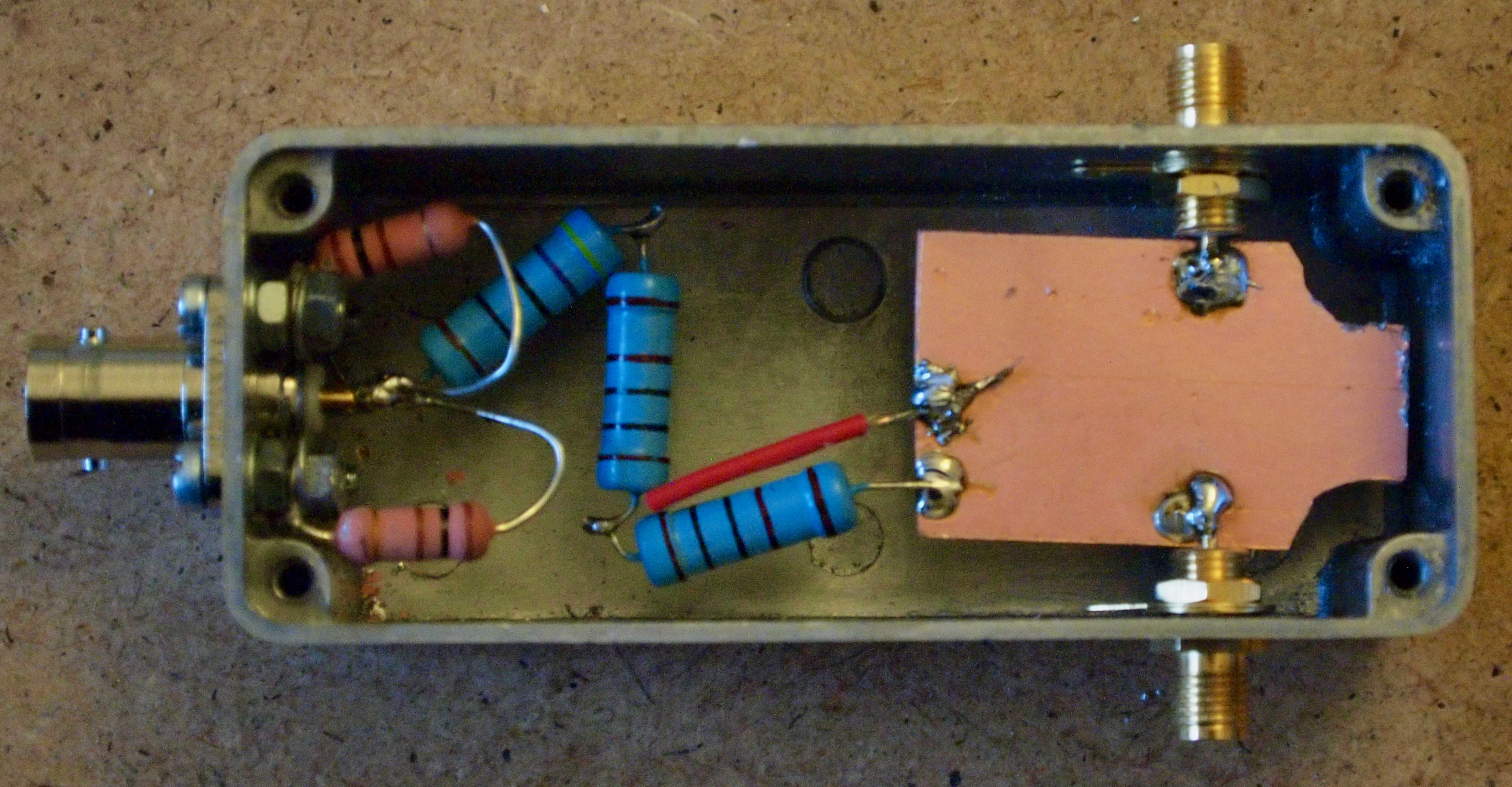 Image 48: Completed RF-tap (©FRS 2018) The large size of the (power) resistors necessited to place the resistors in a zig-zag, which is clearly not an advantage as it will reduce frequency response. Nevertheless, the RF-tap is usable up to about 450 MHz. Tuning and Tests VCO performance For testing the VCO performance a setup was made of the VCO connected with an attenuator (set at -5 dB for matching the input sensitivity of the pre-amp), a pre-amp with a maximum output of 2W (33dBm) at 10 MHz, but here about 1.6W at 400 MHz, the RF-tap, a dump resistor of 50Ω and a 500 MHz bandwidth digital oscilloscope connected to the -40dB side of the tap (image 49):  Image 49: VCO test setup (©FRS 2018) The VCO was set for operating with module VCO2 at a frequency of 400,321.4 kHz (or 400.3 MHz) and the vertical voltage base sensitivity for the scope was 200 mV/div., the horizontal time base sensitivity was 1.00 ns/div. The sinus signal from the VCO measured vertically 450 mV (after - 40 dB attenuation) and the peak to peak time measured a time period of 2.5 ns, which equals a frequency of 400 MHz. This means that the VCO (at the tested frequency of 400 MHz) is sufficiently accurate, stable and therefore suitable for our purposes.  Experimental Setup Prior to integrating the ion source into the Fusor gas line we decided to make an experimental setup in order to find optimal performance. As test gas we used relatively cheap 100% pure Argon welding gas from a non-refillable (throw-away) bottle (image 50) connected to a pressure reducer (image 51): 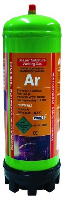  Image 50: gas bottle Image 51: pressure reducing valve The gas flow from the Argon bottle should ideally be around 25 psi (1.7 bar) for feeding a Tylan series 2900 mass flow controller (MFC) as shown in image 52:  Image 52: Tylan FC2901 (Source: supplier) This MFC is a Tylan FC2901 MEP 4V Metal model with a calibration for Argon gas up to a maximum flow of 200 SCCM, which is a maximum flow of 200 ml/min at 0ºC and an air pressure of 760 mm Hg. The connectors for gas inlet and outlet are ¼" VCR male. The flow through the MFC is adjustable between 0 to 100% by means of applying a variable voltage of 0 to 5 VDC. This means that we can make a flow readout box for controlling the MFC. By means of a 10 turns potentiometer we can make a fine adjustment of the voltage varying between 0 and 5 VDC. A dual voltage of ±15 VDC is required for fully opening or closing the MFC. This is required for flushing the system with the working gas, in our test this will be Argon gas and for final use in the Fusor it is Deuterium gas. Normally for flushing purposes a 3-way valve is required to blow off the flushing gas. In our setup this is not essential and we will use a straight line gas supply for both flushing and operation. This is possible because we can pump off the flushing gas during the start up phase of the Fusor when evacuating the Fusor reactor with the roughing vacuum pump. The MFC has two pneumatically operated Swagelok/Nupro SS-BNV51-C bellows valves (image 53) one placed before and one after the MFC.  Image 53: Swagelok/Nupro SS-BNV51-C Pneumatic Bellows Valve (Source: Supplier)
These two valves before and after the MFC are required because the MFC is not totally leakproof and in the closed position may leak gas. The two pneumatic bellows valves prevent this leakage, which is absolutely an important safety issue when working with Deuterium gas. The two pneumatic bellows valves (image 54) are controlled by two 3-way/2-positions pneumatic solenoid controllers operated at 12 - 20 VDC, suitable for connection to our 15 VDC power supply.  Image 54: 3Way/2Position Pneumatic Controller 12VDC (Source: Supplier) The connector on top of the MFC is a 2-row 15-pin DB15 connector (image 55) which has the following functions connected to the pins, including a listung of the wire colors that we have applied to these pins (table 2):
Table 2: pin layout MFC DB15 connector  Image 55: D-sub 15 pin male connector The general idea is to make a flow read out box ourselves on the basis of an Arduino Nano, a 10 turns potentiometer, a power supply, a DC-DC converter, an LCD-display, some switches and a pushbutton. As a power supply we need dual voltage (±) 15 VDC and 0 to 5 VDC for the setpoint of the MFC. The dual 15 VDC is taken from a Mean Well power supply with dimensions of roughly 10x10x4 cm (image 56): 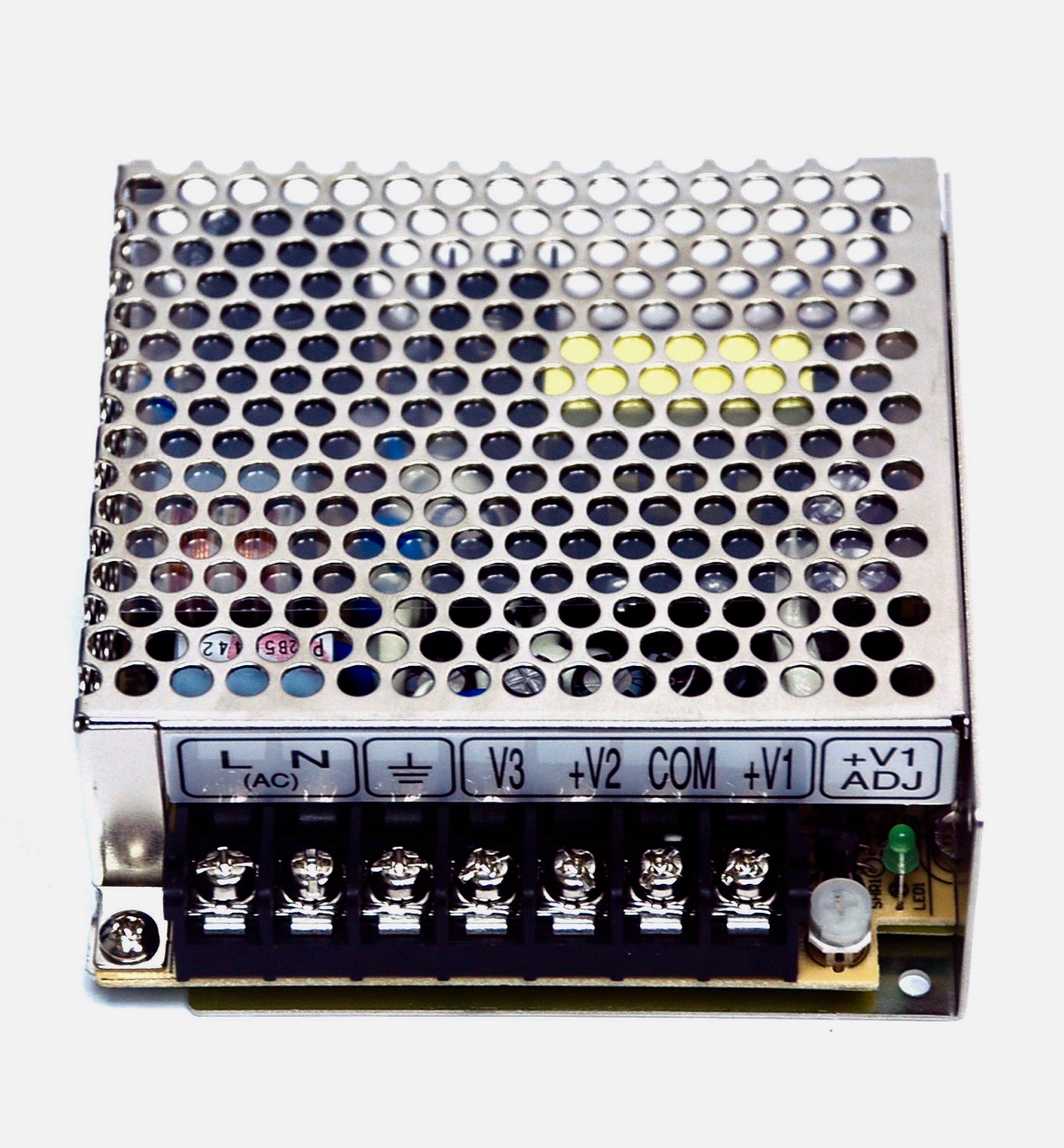 Image 56: Mean Well Power Supply (Source: Supplier) This power supply has AC 100-240V 50/60Hz input and as output on V1 +5VDC 2.5A, on V2 +15VDC 1.0A and on V3 -15VDC 0.5A. For power supply to the Arduino Nano we need 9VDC, which will be obtained from a DC-DC converter which accepts 2.5 to 15VDC input and converts to a stable 9VDC 600mA output (image 57):  Image 57: DC-DC converter (Source: Supplier) The Arduino Nano (image 58) accepts on Vin (pin 30) voltages ranging from 6 to 20 VDC but above 12 VDC the risk exists to burn out the onboard voltage regulalor. Therefore we decided to maximize the input voltage to 9VDC. Another power supply possibility to the Nano is to take directly 5 VDC from the Mean Well power supply and feed it to the 5V or the Vcc pin 27 on the Nano board. In this case we need to adjust the 5VDC voltage output from the Mean Well power supply accurately (use scope) with the potentiometer marked as "+ V1 Adjust". 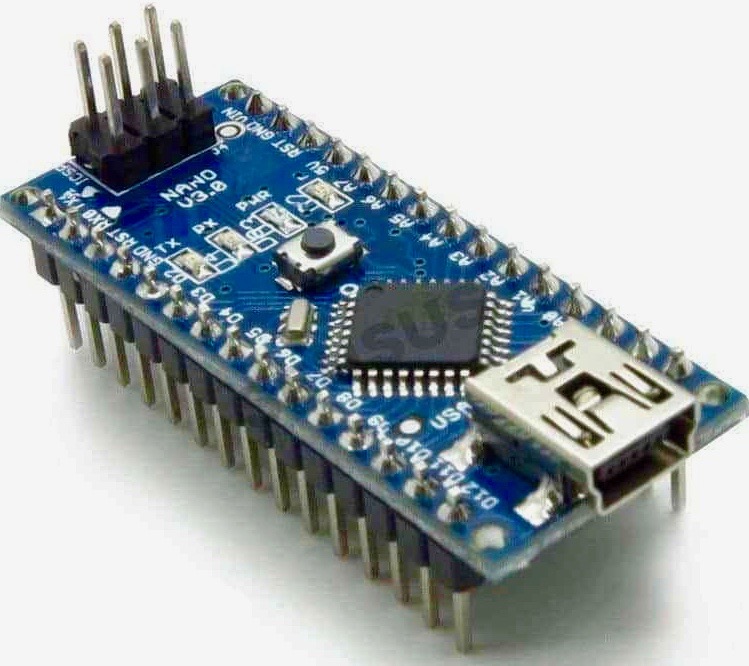 Image 58: Arduino Nano (source Supplier) The Arduino Nano v3 has a compatible ATmega328 Board with a CH340 USB Chip and will be used to drive an LCD display and to control the MFC. (text in progress) |
||||||||||||||||||||||||||||||||||||||||||||||||||||||||||||||||||||||||||||||||||||||||||||||||||
 |
 |
 |
 |
 |
 |
 |
 |
 |
 |
 |
 |
 |
 |
Last Updated on: Mon May 7 23:29:22 2018 |